Atomic Movies May Help Explain Why Perovskite Solar Cells Are More Efficient
SLAC’s ultrafast 'electron camera' reveals unusual atomic motions that could be crucial for the efficiency of next-generation perovskite solar cells.
Menlo Park, Calif. — In recent years, perovskites have taken the solar cell industry by storm. They are cheap, easy to produce and very flexible in their applications. Their efficiency at converting light into electricity has grown faster than that of any other material – from under four percent in 2009 to over 20 percent in 2017 – and some experts believe that perovskites could eventually outperform the most common solar cell material, silicon. But despite their popularity, researchers don’t know why perovskites are so efficient.
Now experiments with a powerful “electron camera” at the Department of Energy’s SLAC National Accelerator Laboratory have discovered that light whirls atoms around in perovskites, potentially explaining the high efficiency of these next-generation solar cell materials and providing clues for making better ones.
“We’ve taken a step toward solving the mystery,” said Aaron Lindenberg from the Stanford Institute for Materials and Energy Sciences (SIMES) and the Stanford PULSE Institute for ultrafast science, which are jointly operated by Stanford University and SLAC. “We recorded movies that show that certain atoms in a perovskite respond to light within trillionths of a second in a very unusual manner. This may facilitate the transport of electric charges through the material and boost its efficiency.”
The study was published today in Science Advances.
Light Sets Atomic Structure in Motion
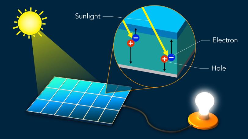
When light shines on a solar cell material, its energy displaces some of the material’s negatively charged electrons. This leaves behind “electron holes” with a positive charge where the electrons were originally located. Electrons and holes migrate to opposite sides of the material, creating a voltage that can be used to power electrical devices.
A solar cell’s efficiency depends on how freely electrons and holes can move in the material. Their mobility, in turn, depends on the material’s atomic structure. In silicon solar cells, for example, silicon atoms line up in a very orderly fashion inside crystals, and even the smallest structural defects reduce the material’s ability to efficiently harvest light.
As a result, silicon crystals must be grown in costly, multistep procedures under extremely clean conditions. In contrast, “Perovskites are readily produced by mixing chemicals into a solvent, which evaporates to leave a very thin film of perovskite material,” said Xiaoxi Wu, the study’s lead author from SIMES at SLAC. “Simpler processing means lower costs. Unlike silicon solar cells, perovskite thin films are also lightweight and flexible and can be easily applied to virtually any surface.”
But what exactly is it about perovskites that allows some of them to harvest light very efficiently? Scientists think that one of the keys is how their atoms move in response to light.
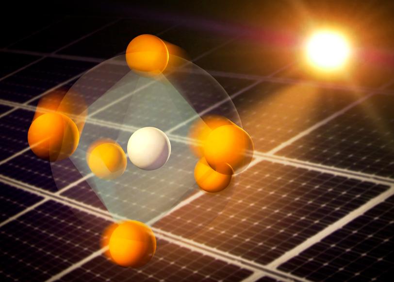
To find out more, Wu and her colleagues studied these motions in a prototype material made of iodine, lead and an organic molecule called methylammonium. The iodine atoms are arranged in octohedra – eight-sided structures that look like two pyramids joined at their bases. The lead atoms sit inside the octohedra and the methylammonium molecules sit between octohedra (see diagram below). This architecture is common to many of the perovskites investigated for solar cell applications.
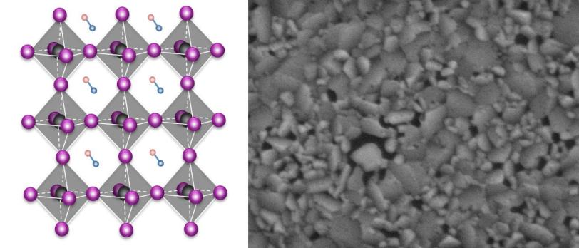
“Previous studies have mostly explored the role of the methylammonium ions and their motions in transporting electric charge through the material,” Wu said. “However, we’ve discovered that light causes large deformations in the network of lead and iodine atoms that could be crucial for the efficiency of perovskites.”
Unusual Distortions May Enhance Efficiency
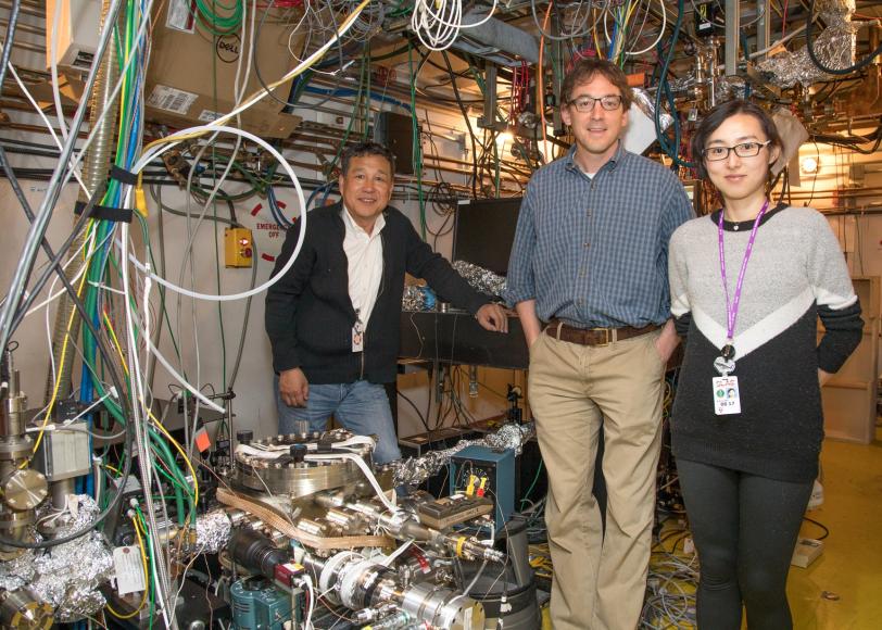
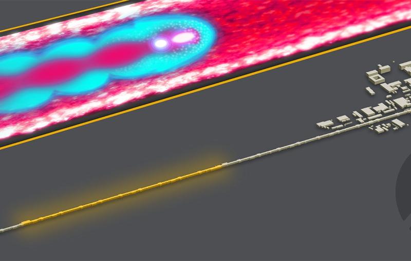
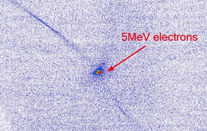
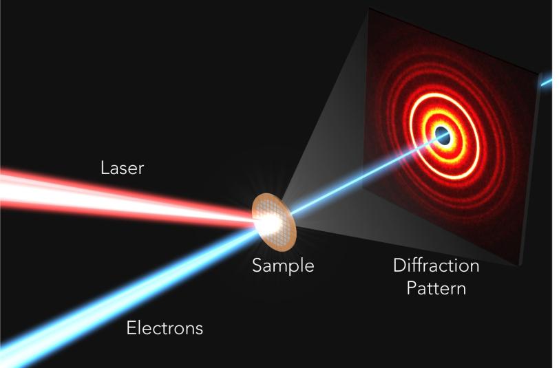
At SLAC’s Accelerator Structure Test Area (ASTA), the researchers first hit a perovskite film, less than two millionths of an inch thick, with a 40-femtosecond laser pulse. One femtosecond is a millionth of a billionth of a second. To determine the atomic response, they sent a 300-femtosecond pulse of highly energetic electrons through the material and observed how the electrons were deflected in the film. This technique, called ultrafast electron diffraction (UED), allowed them to reconstruct the atomic structure.
“By repeating the experiment with different time delays between the two pulses, we obtained a stop-motion movie of the lead and iodine atoms’ motions after the light hit,” said co-author Xijie Wang, SLAC’s lead scientist for UED. “The method is similar to taking a series of ultrafast X-ray snapshots, but electrons give us much stronger signals for thin samples and are less destructive.”
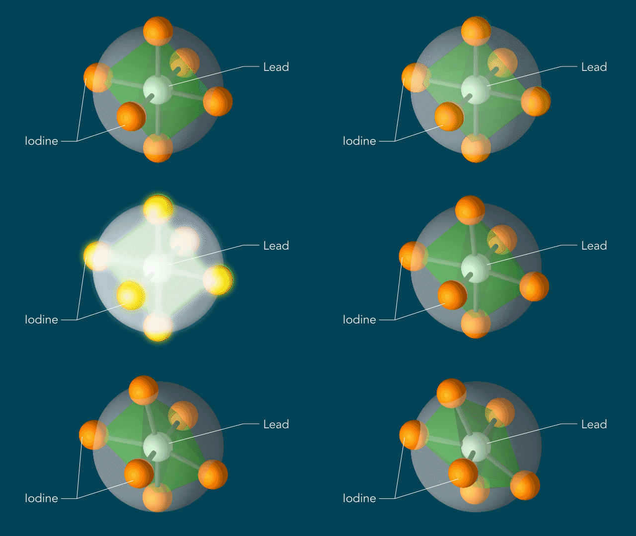
The team expected that the light pulse would affect atoms evenly in all directions, causing them to jiggle around their original positions.
“But that’s not what happened,” Lindenberg said. “Within 10 trillionths of a second after the laser pulse, the iodine atoms rotated around each lead atom as if they were moving on the surface of a sphere with the lead atom at the center, switching each octahedron from a regular shape to a distorted one.”
The surprising deformations were long-lived and unexpectedly large, similar in size to those observed in melting crystals.
“This motion could alter the way charges move,” Wu said. “This response to light could enhance efficiency, for instance by allowing electric charges to migrate through defects and protecting them from being trapped in the material.”
“The results from the Lindenberg group provide fascinating first-time insights into the properties of hybrid perovskites using ultrafast electron diffraction as a unique tool,” according to Felix Deschler, an expert in the field of light-induced physics of novel materials and a researcher at Cambridge University’s Cavendish Lab, who was not involved in the study.
“Knowledge about the detailed atomic motion after photoexcitation yields new information about their performance and can provide new guidelines for material development.”
This work was funded by the DOE Office of Science through SIMES. Other contributors came from the University of Pennsylvania, Columbia University and the Weizmann Institute of Science in Israel.
Written by: Manuel Gnida
Citation: X. Wu et al., Science Advances, 26 July 2017 (10.1126/sciadv.1602388)
Contact
For questions or comments, contact the SLAC Office of Communications at communications@slac.stanford.edu.
SLAC is a multi-program laboratory exploring frontier questions in photon science, astrophysics, particle physics and accelerator research. Located in Menlo Park, California, SLAC is operated by Stanford University for the U.S. Department of Energy Office of Science. To learn more, please visit www.slac.stanford.edu.
SLAC National Accelerator Laboratory is supported by the Office of Science of the U.S. Department of Energy. The Office of Science is the single largest supporter of basic research in the physical sciences in the United States, and is working to address some of the most pressing challenges of our time. For more information, please visit science.energy.gov.
