Scientists Get First Glimpse of Conductivity That Could Break Size Barriers for Memory
Stanford/SLAC Results Confirm Exotic Phenomenon Postulated Decades Ago
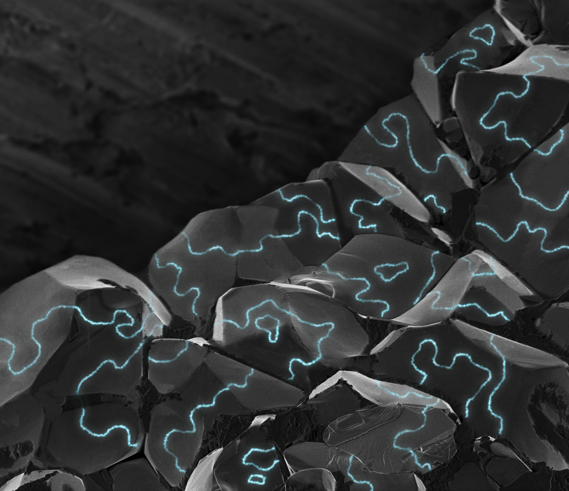
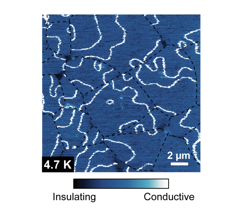
Scientists from Stanford University and the Department of Energy’s SLAC National Accelerator Laboratory have made the first direct images showing that electrical currents can flow along the boundaries between tiny magnetic regions of a material that normally doesn’t conduct electricity. The results could have major implications for magnetic memory storage.
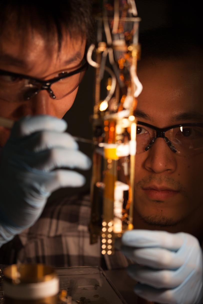
"This can provide a more straightforward way to use magnetic material as memory,” said Eric Yue Ma, a graduate student in the laboratory of Zhi-Xun Shen, the SLAC and Stanford professor who led the research. “Today you need to convert magnetic information into electrical information when reading magnetic memory, usually via multiple layers of different materials. But if you have both types of information within the material itself, you can skip that step.”
The team has filed a provisional patent on the concept of using this phenomenon to make new types of sensors and very stable, high-density memory storage that can potentially go beyond the size limitations of current technologies. They report the results of their study today in the journal Science.
Unconventional Times Two
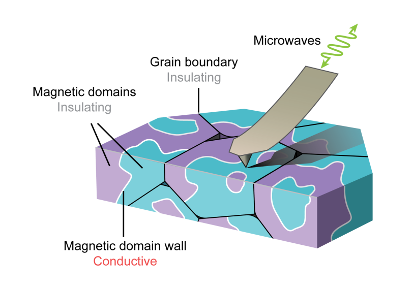
The material they studied, which was synthesized by researchers at the University of Tokyo and the RIKEN research institution in Japan, is relatively new – a combination of neodymium, iridium and oxygen. It’s magnetic, but not in the conventional sense. Although it consists of microscopic regions, or “domains,” where the spins of electrons line up and generate tiny magnetic fields, in this case the fields all cancel each other out. So the material as a whole has zero magnetism and would not stick to your fridge.
The material doesn’t conduct electricity, either, in a conventional way. But theorists have postulated and argued since the 1950s that this type of material, known as a magnetic insulator, might conduct electrical current along the boundaries between its magnetic domains.
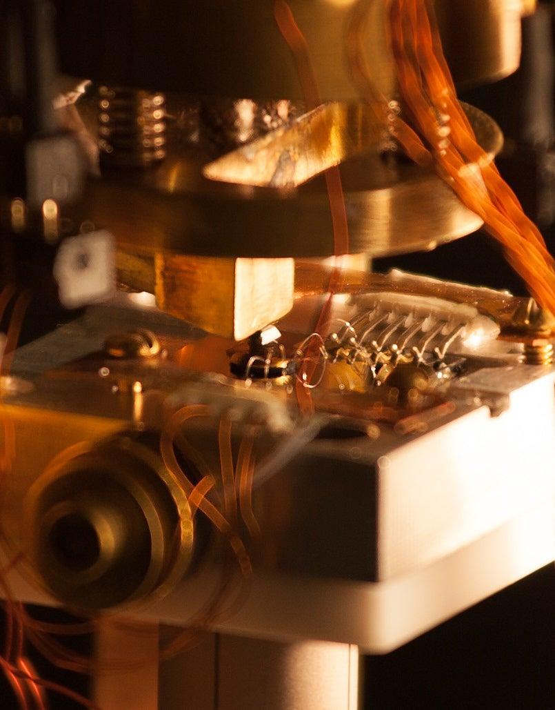
Shen’s group used a technique they invented to directly image those boundaries and show they are electrically conductive – as if they were thin ribbons of aluminum foil snaking through an insulating slab of glass. The technique is called microwave impedance microscopy, or MIM. It sends microwaves down through the tip of a probe that is in direct contact with the material, and collects the microwave signals that are reflected back. This allows them to measure the electrical resistance of the material – how well it conducts electricity – in areas as small as 100 nanometers, or billionths of a meter. Shen recently received one of the top grants in quantum materials research from the Gordon and Betty Moore Foundation to develop the next generation of MIM.
“This physics is interesting and had been thought to exist, but it remained elusive for the last 60 years,” Shen said. “Now it’s been seen directly in this experiment.”
A Beautiful Technique
Leon Balents, a professor of physics at the University of California, Santa Barbara who was not involved in the study, said the results were impressive.
“It’s a beautiful experimental technique, to be able to make these measurements, and the technique could be applied to a huge range of materials,” he said. “It’s remarkable how large the magnetic domains are. That’s great news; it means we can isolate a single domain and measure its properties. And now that they have a handle on being able to locate the domains, they can use those techniques to attack further questions.
“While this is a fundamental physics study,” he said, “in the long term people are thinking toward many different types of applications.”
Future Devices and Studies
In a provisional U.S. patent application filed by Stanford and RIKEN, the inventors suggest that manipulating the arrangement of the magnetic domains in these materials could offer a way to store information. Changing the number of domains within a small area by applying heat or strain, for instance, could make it dramatically more insulating or conductive. These two sharply contrasting states could be directly read as ones and zeroes and used to store and retrieve information. The resulting memory devices should be more stable than today’s FLASH memory, “potentially holding data practically permanently,” the inventors wrote. More importantly, such devices can potentially be scaled down below the fundamental size limits for FLASH set by semiconductor physics to make the memories of the future.
Although the material studied here could harbor domain boundary conductivity only at extremely cold temperatures, the team pointed out that other scientists have recently reported signs of similar properties in a material that could work at a much warmer temperature of minus 45 degrees Fahrenheit.
Shen’s group is working to improve the resolution of their MIM technique for studies of these and other materials with potential for creating entirely new types of devices.
In addition to SLAC and Stanford, other collaborators in the study were from the University of Tokyo and the Center for Emergent Matter Science at RIKEN in Japan; the Center for Advancing Materials Performance from the Nanoscale at Xi’an Jiaotong University and Shanghai Institute of Microsystem and Information Technology in China; and the Advanced Light Source, a DOE Office of Science User Facility at Lawrence Berkeley National Laboratory. The MIM measurements at Stanford were supported by the National Science Foundation and the Gordon and Betty Moore Foundation.
Citation: E. Ma et al., Science, 30 October 2015 (10.1126/science.aac8289)
For questions or comments, contact the SLAC Office of Communications at communications@slac.stanford.edu.
SLAC is a multi-program laboratory exploring frontier questions in photon science, astrophysics, particle physics and accelerator research. Located in Menlo Park, Calif., SLAC is operated by Stanford University for the U.S. Department of Energy's Office of Science.
SLAC National Accelerator Laboratory is supported by the Office of Science of the U.S. Department of Energy. The Office of Science is the single largest supporter of basic research in the physical sciences in the United States, and is working to address some of the most pressing challenges of our time. For more information, please visit science.energy.gov.
