Researchers control quantum properties of 2D materials with tailored light
The team developed a groundbreaking method that harnesses the structure of light to twist and tweak the properties of quantum materials.
A team of scientists has developed a groundbreaking method that harnesses the structure of light to twist and tweak the properties of quantum materials. Their results, published today in Nature, pave the way for advancements in next generation quantum electronics, quantum computing and information technology.
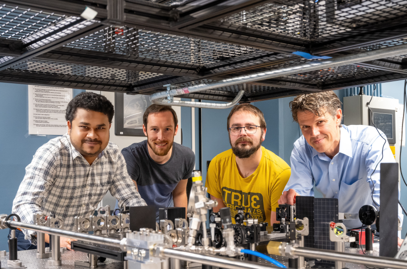
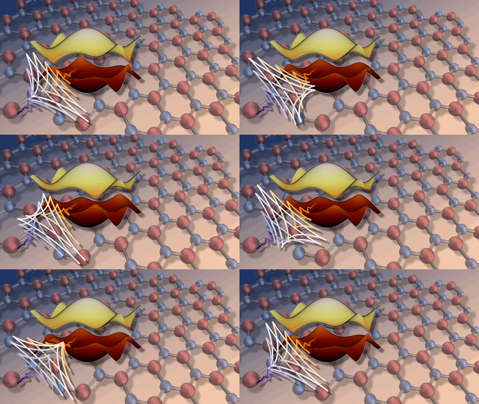
The team, led by researchers from the Department of Energy’s SLAC National Accelerator Laboratory and Stanford University, applied this method to a material known as hexagonal boron nitride (hBN), a single layer of atoms arranged in a honeycomb pattern with properties that make it uniquely suited for quantum manipulation. In their experiments, the scientists used a special kind of light, whose electric field looks like a trefoil, to change and control the material's behavior on a quantum level at an ultrafast time scale.
The way the light wave is twisted also allows researchers to precisely control the material's quantum properties – rules that determine the behavior of electrons, which are essential for electricity and data flow. This ability to control quantum properties on demand could pave the way for creating ultrafast quantum switches for future technologies.
"Our work is akin to finding a new way of whispering to the quantum world and getting it to reveal its secrets to us," said Shubhadeep Biswas, a scientist at SLAC and Stanford University who led the research.
Traditional techniques often require the light to have just the right energy to work with a material, a limitation that this new approach cleverly bypasses. By using a special kind of light and tailoring its pattern to match the material's pattern, scientists can coax the material into new configurations without being constrained by its natural properties.
"This structured light doesn't just illuminate the material; it twists around it, altering its quantum properties on demand in a way we can control," Biswas said.
This flexibility could allow the method to work for a broad range of applications, making it easier to develop new technologies. In essence, the team created conditions where electrons move in new and controllable ways. That could, for example, lead to the development of super-fast switches for quantum computers, which could drastically outperform the computers we use today.
Beyond the immediate results, this research holds promise for future applications in the realm of "valleytronics," a field that leverages the quantum properties of electrons residing in different energy valleys of a material for information processing. Unlike traditional approaches that require light matched to those energy valleys, the new method is more adaptable, offering a new direction for developing quantum devices.
The researchers' ability to manipulate the quantum valleys in hBN could lead to new devices, such as ultrafast quantum switches, that operate not just on the binary of 0s and 1s but on the more complex landscape of quantum information. This will allow for faster, more efficient ways of processing and storing information.
"It’s not just about flipping a switch on and off," said collaborator Matthias F. Kling, the R&D division director at LCLS. "It's about creating a switch that can exist in multiple states at once, vastly increasing the power and potential of our devices. It opens up a whole new way to engineer the properties of materials on a quantum level. The potential applications are vast, ranging from quantum computing to new forms of quantum information processing."
The research also sheds light on the fundamental ways scientists can interact with and control the quantum world. For the scientists involved, this journey into the quantum realm is not just about the thrill of discovery but about pushing the boundaries of what's possible.
"One of the most exciting aspects is the sheer potential of our findings,” Biswas said. “We're on the cusp of a new era in technology, and we're just starting to explore what's possible when we harness the power of quantum materials."
LCLS is a DOE Office of Science user facility. This research was supported by the Office of Science. The team also included researchers from Max Planck Institute of Quantum Optics, Garching; Ludwig-Maximilians-Universitat Munich in Germany; and Instituto de Ciencia de Materiales de Madrid in Spain.
Citation: S. Mitra et al., Nature, 15 March 2024 (10.1038/s41586-024-07244-z)
Contact
For questions or comments, contact the SLAC Office of Communications at communications@slac.stanford.edu.
About SLAC
SLAC National Accelerator Laboratory explores how the universe works at the biggest, smallest and fastest scales and invents powerful tools used by researchers around the globe. As world leaders in ultrafast science and bold explorers of the physics of the universe, we forge new ground in understanding our origins and building a healthier and more sustainable future. Our discovery and innovation help develop new materials and chemical processes and open unprecedented views of the cosmos and life’s most delicate machinery. Building on more than 60 years of visionary research, we help shape the future by advancing areas such as quantum technology, scientific computing and the development of next-generation accelerators.
SLAC is operated by Stanford University for the U.S. Department of Energy’s Office of Science. The Office of Science is the single largest supporter of basic research in the physical sciences in the United States and is working to address some of the most pressing challenges of our time.
